| [ Team LiB ] |
|
Electrical CharacteristicsAt its heart, a microprocessor is an electronic device. This electronic foundation has important ramifications in the construction and operation of chips. The "free lunch" principle (that is, there is none) tells us that every operation has its cost. Even the quick electronic thinking of a microprocessor takes a toll. The thinking involves the switching of the state of tiny transistors, and each state change consumes a bit of electrical power, which gets converted to heat. The transistors are so small that the process generates a minuscule amount of heat, but with millions of them in a single chip, the heat adds up. Modern microprocessors generate so much heat that keeping them cool is a major concern in their design. Thermal ConstraintsHeat is the enemy of the semiconductor because it can destroy the delicate crystal structure of a chip. If a chip gets too hot, it will be irrevocably destroyed. Packing circuits tightly concentrates the heat they generate, and the small size of the individual circuit components makes them more vulnerable to damage. Heat can cause problems more subtle than simple destruction. Because the conductivity of semiconductor circuits also varies with temperature, the effective switching speed of transistors and logic gates also changes when chips get too hot or too cold. Although this temperature-induced speed change does not alter how fast a microprocessor can compute (the chip must stay locked to the system clock at all times), it can affect the relative timing between signals inside the microprocessor. Should the timing get too far off, a microprocessor might make a mistake, with the inevitable result of crashing your system. All chips have rated temperature ranges within which they are guaranteed to operate without such timing errors. Because chips generate more heat as speed increases, they can produce heat faster than it can radiate away. This heat buildup can alter the timing of the internal signals of the chip so drastically that the microprocessor will stop working andas if you couldn't guesscause your system to crash. To avoid such problems, computer manufacturers often attach heatsinks to microprocessors and other semiconductor components to aid in their cooling. A heatsink is simply a metal extrusion that increases the surface area from which heat can radiate from a microprocessor or other heat-generating circuit element. Most heatsinks have several fins (rows of pins) or some geometry that increases its surface area. Heatsinks are usually made from aluminum because that metal is one of the better thermal conductors, enabling the heat from the microprocessor to quickly spread across the heatsink. Heatsinks provide passive cooling (passive because cooling requires no power-using mechanism). Heatsinks work by convection, transferring heat to the air that circulates past the heatsink. Air circulates around the heatsink because the warmed air rises away from the heatsink and cooler air flows in to replace it. In contrast, active cooling involves some kind of mechanical or electrical assistance to remove heat. The most common form of active cooling is a fan, which blows a greater volume of air past the heatsink than would be possible with convection alone. Nearly all modern microprocessors require a fan for active cooling, typically built into the chip's heatsink. The makers of notebook computers face another challenge in efficiently managing the cooling of their computers. Using a fan to cool a notebook system is problematic. The fan consumes substantial energy, which trims battery life. Moreover, the heat generated by the fan motor itself can be a significant part of the thermal load of the system. Most designers of notebook machines have turned to more innovative passive thermal controls, such as heat pipes and using the entire chassis of the computer as a heatsink. Operating VoltagesIn desktop computers, overheating rather than excess electrical consumption is the major power concern. Even the most wasteful of microprocessors uses far less power than an ordinary light bulb. The most that any computer-compatible microprocessor consumes is about nine watts, hardly more than a night light and of little concern when the power grid supplying your computer has megawatts at its disposal. If you switch to battery power, however, every last milliwatt is important. The more power used by a computer, the shorter the time its battery can power the system or the heavier the battery it will need to achieve a given life between charges. Every degree a microprocessor raises its case temperature clips minutes from its battery runtime. Battery-powered notebooks and sub-notebook computers consequently caused microprocessor engineers to do a quick about-face. Whereas once they were content to use bigger and bigger heatsinks, fans, and refrigerators to keep their chips cool, today they focus on reducing temperatures and wasted power at the source. One way to cut power requirements is to make the design elements of a chip smaller. Smaller digital circuits require less power. But shrinking chips is not an option; microprocessors are invariably designed to be as small as possible with the prevailing technology. To further trim the power required by microprocessors to make them more amenable to battery operation, engineers have come up with two new design twists: low-voltage operation and system-management mode. Although founded on separate ideas, both are often used together to minimize microprocessor power consumption. All new microprocessor designs incorporate both technologies. Since the very beginning of the transistor-transistor logic family of digital circuits (the design technology that later blossomed into the microprocessor), digital logic has operated with a supply voltage of 5 volts. That level is essentially arbitrary. Almost any voltage would work. But 5-volt technology offers some practical advantages. It's low enough to be both safe and frugal with power needs but high enough to avoid noise and allow for several diode drops, the inevitable reduction of voltage that occurs when a current flows across a semiconductor junction. Every semiconductor junction, which essentially forms a diode, reduces or drops the voltage flowing through it. Silicon junctions impose a diode drop of about 0.7 volts, and there may be one or more such junctions in a logic gate. Other materials impose smaller dropsthat of germanium, for example, is 0.4 voltsbut the drop is unavoidable. There's nothing magical about using 5 volts. Reducing the voltage used by logic circuits dramatically reduces power consumption because power consumption in electrical circuits increases by the square of the voltage. That is, doubling the voltage of a circuit increases the power it uses by fourfold. Reducing the voltage by one-half reduces power consumption by three-quarters (providing, of course, that the circuit will continue to operate at the lower voltage). All current microprocessor designs operate at about 2 volts or less. The Pentium 4 operates at just over 1.3 volts with minor variations, depending on the clock frequency of the chip. For example, the 2.53GHz version requires 1.325 volts. Microprocessors designed for mobile applications typically operate at about 1.1 volts; some as low as 0.95 volt. To minimize power consumption, Intel sets the operating voltage of the core logic of its chips as low as possiblesome, such as Intel's ultra-low-voltage Mobile Pentium III-M, to just under 1 volt. The integral secondary caches of these chips (which are fabricated separately from the core logic) usually require their own, often higher, voltage supply. In fact, operating voltage has become so critical that Intel devotes several pins of its Pentium II and later microprocessors to encoding the voltage needs of the chip, and the host computer must adjust its supply to the chip to precisely meet those needs. Most bus architectures and most of today's memory modules operate at the 3.3 volt level. Future designs will push that level lower. Rambus memory systems, for example, operate at 2.5 volts (see Chapter 6, "Chipsets," for more information). Power ManagementTrimming the power need of a microprocessor both reduces the heat the chip generates and increases how long it can run off a battery supply, an important consideration for portable computers. Reducing the voltage and power use of the chip is one way of keeping the heat down and the battery running, but chipmakers have discovered they can save even more power through frugality. The chips use power only when they have to, thus managing their power consumption. Chipmakers have two basic power-management strategies: shutting off circuits when they are not needed and slowing down the microprocessor when high performance is not required. The earliest form of power-savings built into microprocessors was part of system management mode (SMM), which allowed the circuitry of the chip to be shut off. In terms of clock speed, the chip went from full speed to zero. Initially, chips switched off after a period of system inactivity and woke up to full speed when triggered by an appropriate interrupt. More advanced systems cycled the microprocessor between on and off states as they required processing power. The chief difficulty with this design is that nothing gets done when the chip isn't processing. This kind of power management only works when you're not looking (not exactly a salesman's dream) and is a benefit you should never be able to see. Intel gives this technique the name QuickStart and claims that it can save enough energy between your keystrokes to significantly reduce overall power consumption by briefly cutting the microprocessor's electrical needs by 95 percent. Intel introduced QuickStart in the Mobile Pentium II processor, although it has not widely publicized the technology. In the last few years, chipmakers have approached the power problem with more advanced power-saving systems that take an intermediary approach. One way is to reduce microprocessor power when it doesn't need it for particular operations. Intel slightly reduces the voltage applied to its core logic based on the activity of the processor. Called Intel Mobile Voltage Positioning (IMVP), this technology can reduce the thermal design powerwhich means the heat produced by the microprocessorby about 8.5 percent. According to Intel, this reduction is equivalent to reducing the speed of a 750MHz Mobile Pentium III by 100MHz. Another technique for saving power is to reduce the performance of a microprocessor when its top speed is not required by your applications. Instead of entirely switching off the microprocessor, the chipmakers reduce its performance to trim power consumption. Each of the three current major microprocessor manufacturers puts its own spin on this performance-as-needed technology, labeling it with a clever trademark. Intel offers SpeedStep, AMD offers PowerNow!, and Transmeta offers LongRun. Although at heart all three are conceptually much the same, in operation you'll find distinct differences between them. Intel SpeedStepInternal mobile microprocessor power savings started with SpeedStep, introduced by Intel on January 18, 2000, with the Mobile Pentium III microprocessors, operating at 600MHz and 650MHz. To save power, these chips can be configured to reduce their operating speed when running on battery power to 500MHz. All Mobile Pentium III and Mobile Pentium 4 chips since that date have incorporated SpeedStep into their designs. Mobile Celeron processors do not use SpeedStep. The triggering event is a reduction of power to the chip. For example, the initial Mobile Pentium III chips go from the 1.7 volts that is required for operating at their top speeds to 1.35 volts. As noted earlier, the M-series step down from 1.4 to 1.15 volts, the low-voltage M-series from 1.35 to 1.1 volts, and the ultra-low-voltage chips from 1.1 to 0.975 volts. Note that a 15-percent reduction in voltage in itself reduces power consumption by about 29 percent, with a further reduction that's proportional to the speed decrease. The 600MHz Pentium III, for example, cuts its power consumption an additional 17 percent thanks to voltage reduction when slipping down from 600MHz to 500MHz. Intel calls the two modes Maximum Performance Mode (for high speed) and Battery Optimized Mode (for low speed). According to Intel, switching between speeds requires about one two-thousandths of a second. The M-series of Mobile Pentium III adds an additional step to provide an intermediary level of performance when operating on battery. Intel calls this technology Enhanced SpeedStep. Table 5.1 lists the SpeedStep capabilities of many Intel chips. AMD PowerNow!Advanced Micro Devices devised its own power-saving technology, called PowerNow!, for its mobile processors. The AMD technology differs from Intel's SpeedStep by providing up to 32 levels of speed reduction and power savings. Note that 32 levels is the design limit. Actual implementations of the technology from AMD have far fewer levels. All current AMD mobile processorsboth the Mobile Athlon and Mobile Duron linesuse PowerNow! technology. PowerNow! operates in one of three modes:
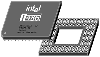
The actual means of varying the clock frequency involves dynamic control of the clock multiplier inside the AMD chip. The external oscillator or clock frequency the computer supplies the microprocessor does not change, regardless of the performance demand. In the case of the initial chip to use PowerNow! (the Mobile K6-2+ chip, operating at 550MHz), its actual operating speed could vary from 200MHz to 550MHz in a system that takes full advantage of the technology. Control of PowerNow! starts with the operating system (which is almost always Windows). Windows monitors processor usage, and when it dips below a predetermined level, such as 50 percent, Windows signals the PowerNow! system to cut back the clock multiplier inside the microprocessor and then signals a programmable voltage regulator to trim the voltage going to the chip. Note that even with PowerNow!, the chip's supply voltage must be adjusted externally to the chip to achieve the greatest power savings. If the operating system detects that the available processing power is still underused, it signals to cut back another step. Similarly, should processing needs reach above a predetermined level (say, 90 percent of the available ability), the operating system signals PowerNow! to kick up performance (and voltage) by a notch. Transmeta LongRunTransmeta calls its proprietary power-saving technology LongRun. It is a feature of both current Crusoe processors, the TM5500 and TM5800. In concept, LongRun is much like AMD's PowerNow! The chief difference is control. Because of the design of Transmeta's Crusoe processors, Windows instructions are irrelevant to their power usageCrusoe chips translate the Windows instructions into their own format. To gauge its power needs, the Crusoe chip monitors the flow of its own native instructions and adjusts its speed to match the processing needs of that code stream. In other words, the Crusoe chip does its own monitoring and decision-making regarding power savings without regard to Windows power-conservation information. According to Transmeta, LongRun allows its microprocessors to adjust their power consumption by changing their clock frequency on the fly, just as PowerNow! does, as well as to adjust their operating voltage. The processor core steps down processor speed in 33MHz increments, and each step holds the potential of reducing chip voltage. For example, trimming the speed of a chip from 667MHz to 633MHz also allows for reducing the operating voltage from 1.65 to 1.60 volts. PackagingThe working part of a microprocessor is exactly what the nickname "chip" implies: a small flake of a silicon crystal no larger than a postage stamp. Although silicon is a fairly robust material with moderate physical strength, it is sensitive to chemical contamination. After all, semiconductors are grown in precisely controlled atmospheres, the chemical content of which affects the operating properties of the final chip. To prevent oxygen and contaminants in the atmosphere from adversely affecting the precision-engineered silicon, the chip itself must be sealed away. The first semiconductors, transistors, were hermetically sealed in tiny metal cans. The art and science of semiconductor packaging has advanced since those early days. Modern integrated circuits (ICs) are often surrounded in epoxy plastic, an inexpensive material that can be easily molded to the proper shape. Unfortunately, microprocessors can get very hot, sometimes too hot for plastics to safely contain. Most powerful modern microprocessors are consequently cased in ceramic materials that are fused together at high temperatures. Older, cooler chips reside in plastic. The most recent trend in chip packaging is the development of inexpensive tape-based packages optimized for automated assembly of circuit boards. The most primitive of microprocessors (that is, those of the early generation that had neither substantial signal nor power requirements) fit in the same style housing popular for other integrated circuitsthe infamous dual inline pin (DIP) package. The packages grew more pinsor legs, as engineers sometimes call themto accommodate the ever-increasing number of signals in data and address buses. The DIP package is far from ideal for a number of reasons. Adding more connections, for example, makes for an ungainly chip. A centipede microprocessor would be a beast measuring a full five inches long. Not only would such a critter be hard to fit onto a reasonably sized circuit board, it would require that signals travel substantially farther to reach the end pins than those in the center. At modern operating frequencies, that difference in distance can amount to a substantial fraction of a clock cycle, potentially putting the pins out of sync. Modern chip packages are compact squares that avoid these problems. Engineers developed several separate styles to accommodate the needs of the latest microprocessors. The most common is the pin grid array (PGA), a square package that varies in size with the number of pins that it must accommodate (typically about two inches square). The first PGA chips had 68 pins. Pentium 4 chips in PGA packages have up to 478. No matter their number, the pins are spaced as if they were laid out on a checkerboard, making the "grid array" of the package name (see Figure 5.1). Figure 5.1. Pin-grid array socket (with PGA chip).
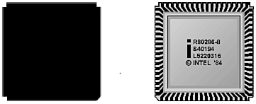
To fit the larger number of pins used by wider-bus microprocessors into a reasonable space, Intel rearranged the pins of some processors (notably the Pentium Pro), staggering them so that they can fit closer together. The result is a staggered pin grid array (SPGA) package, as shown in Figure 5.2. Figure 5.2. A Multi-Cavity Module (MCM) SPGA package.
Pins take up space and add to the cost of fabrication, so chipmakers have developed a number of pinless packages. The first of these to find general use was the Leadless Chip Carrier (LCC) socket. Instead of pins, this style of package has contact pads on one of its surfaces. The pads are plated with gold to avoid corrosion or oxidation that would impede the flow of the minute electrical signals used by the chip (see Figure 5.3). The pads are designed to contact special springy mating contacts in a special socket. Once installed, the chip itself may be hidden in the socket, under a heat sink, or perhaps only the top of the chip may be visible, framed by the four sides of the socket. Figure 5.3. Leadless Chip Carrier microprocessor, top and bottom views.
A related design, the Plastic Leaded Chip Carrier (PLCC), substitutes epoxy plastic for the ceramic materials ordinarily used for encasing chips. Plastic is less expensive and easier to work with. Some microprocessors with low thermal output sometimes use a housing designed to be soldered downthe Plastic Quad Flat Package (PQFP), sometimes called simply the quad flat pack because the chips are flat (they fit flat against the circuit board) and they have four sides (making them a quadrilateral, as shown in Figure 5.4). Figure 5.4. Plastic Quad Flat Package microprocessor.
The Tape Carrier Package takes the advantage of the quad flat pack a step further, reducing the chip to what looks like a pregnant bulge in the middle of a piece of photographic film (see Figure 5.5). Figure 5.5. Tape Carrier Package microprocessor.
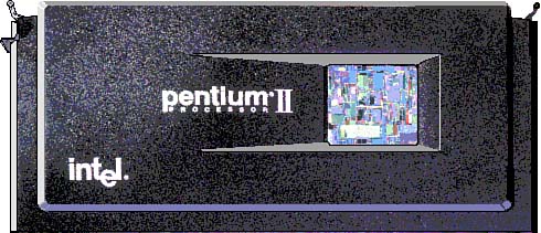
Another way to deal with the problem of pins is to reduce them to vestigial bumps, substituting precision-formed globs of solder that can mate with socket contacts. Alternately, the globs can be soldered directly to a circuit board using surface-mount technology. Because the solder contacts start out as tiny balls but use a variation on the PGA layout, the package is termed solder-ball grid array. (Note that solder is often omitted from the name, thus yielding the abbreviation BGA.) When Intel's engineers first decided to add secondary caches to the company's microprocessors, they used a separately housed slice of silicon for the cache. Initially Intel put the CPU and cache chips in separate chambers in one big, black chip. The design, called the Multi-Cavity Module (MCM), was used only for the Pentium Pro chip. Next, Intel shifted to putting the CPU and cache on a small circuit board inside a cartridge, initially called the Single Edge Contact cartridge or SEC cartridge (which Intel often abbreviates SECC) when it was used for the Pentium II chip. Figure 5.6 shows the Pentium II microprocessor SEC cartridge. Figure 5.6. The SEC cartridge as used in the Intel Pentium II.
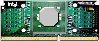
Intel used a functionally similar but physically different design for its Pentium II Xeon chips and a similar cartridge but slightly different bus design for the Pentium III. To cut the cost of the cartridge for the inexpensive Celeron line, Intel eliminated the case around the chip to make the Singe-Edge Processor (SEP) package (see Figure 5.7). Figure 5.7. The SEP package as used by the Intel Celeron micro-processor.
When Intel developed the capability to put the CPU and secondary cache on a single piece of silicon, called a die, the need for cartridges disappeared. Both later Celeron and Pentium III had on-die caches and were packaged both as cartridges and as individual chips in PGA and similar packages. With the Pentium 4, the circle was complete. Intel offers the latest Pentiums only in compact chip-style packages. The package that the chip is housed in has no effect on its performance. It can, however, be important when you want to replace or upgrade your microprocessor with a new chip or upgrade card. Many of these enhancement products require that you replace your system's microprocessor with a new chip or adapter cable that links to a circuit board. If you want the upgrade or a replacement part to fit on your motherboard, you may have to specify which package your computer uses for its microprocessor. Ordinarily you don't have to deal with microprocessor sockets unless you're curious and want to pull out the chip, hold it in your hand, and watch a static discharge turn a $300 circuit into epoxy-encapsulated sand. Choose to upgrade your computer to a new and better microprocessor, and you'll tangle with the details of socketry, particularly if you want to improve your Pentium. Intel recognizes nine different microprocessor sockets for its processors, from the 486 to the Pentium Pro. In 1999, it added a new socket for some incarnations of the Pentium II Celeron. Other Pentium II and Pentium III chips, packaged as modules or cartridges, mate with slots instead of sockets. Table 5.2 summarizes these socket types, the chips that use them, and the upgrades appropriate to them. |
| [ Team LiB ] |
|